
This text describes in detail how, when and why the V9938 reads from and writes to VRAM in bitmap screen modes (screen 5, 6, 7 and 8). VRAM is accessed for bitmap and sprite rendering but also for VDP command execution or by CPU VRAM read/write requests.
Modern MSX emulators like blueMSX and openMSX are already fairly accurate. And for most practical applications like games or even demos they are already good enough. Though there are cases where you can still clearly see the difference between a real and an emulated MSX machine.
For example the following pictures show the speed of the LINE command for different slopes of the line. The first two pictures are generated on different MSX emulators, the last picture is from a real MSX. Without going into all the details: lines are drawn from the center of the image to each point at the border. While the LINE commands are executing, the command color register is rapidly changed (at a fixed rate). So faster varying colors indicate a slower executing command.


From left to right these pictures show:
This test is derived from NYRIKKI's test program described in this (long) MRC forum thread. This particular test is not that important. But because it generates a nice graphical output it allows to show the problem without going into too much technical details (yet).
In most MSX applications these LINE speed differences, or small command speed differences in general, likely won't cause any problems. (Except of course in programs like this that specifically test for it.) But it would still be nice to improve the emulators.
To be able to improve openMSX further we need to have a good understanding of what it is exactly that causes these irregularities. It would be very hard to figure out this stuff only by using MSX test programs. It might be easier to look at the deeper hardware level. More specifically at the communication between the VDP (V9938) and the VRAM chips. This should allow us to see when exactly the VDP reads or writes which VRAM addresses.
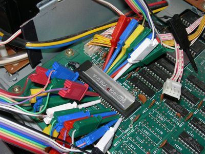
So at the 2013 MSX fair in Nijmegen we (some member of the openMSX team and I) connected a logic analyzer to the VDP-VRAM bus in a Philips NMS8250 machine. The following picture gives an impression of our measurement setup.
Next we ran some MSX software that puts the VDP in a certain display mode. It enables/disables screen and/or sprite rendering. And it optionally executes VDP commands and/or accesses VRAM via the CPU. And while this test was running we could capture (small chunks of) the communication between the VDP and the VRAM. This gives us output (waveforms) like in the following image.
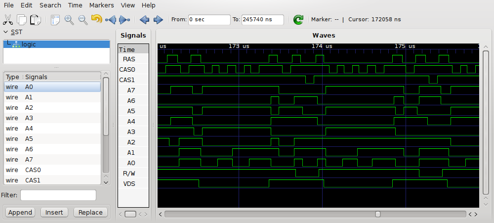
It's not so easy to go from this waveform data to meaningful results about how the VDP operates. This text also won't talk about this analysis process. If you're interested in the analysis or in the raw measurement data, you can find some more details in the openmsx-devel mailinglist archive. The rest of this text will only discuss the final results of the analysis.
Because one of the primary goals was to improve the command engine emulation in openMSX, the measurements mostly focused on the bitmap screen modes (a V9938 doesn't allow commands in non-bitmap modes). So the following sections will only occasionally mention text or character modes. Because we used a V9938 we also couldn't test the YJK modes (screen 11 and 12). But it's highly likely that, from a VRAM access point of view, these modes behave the same as screen 8 (or as we'll see later, the same as all the bitmap screen modes).
Before presenting the actual results of (the analysis of) the measurements, this section first explains the general workings of the VDP-VRAM communication. This is mostly a description of the functional interface of DRAM chips, but then specifically applied to the VDP case. Feel free to skim (or even skip) this section.
Like most RAM chips in MSX machines, the VDP uses DRAM chips for the video RAM. There exist many variations in DRAM chips. You can find a whole lot of information on wikipedia. Most of the info in this section can also be found in the 'V9938 Technical Data Book'. Often that book goes into a lot more detail than this text. Here I highlight (and simplify) the aspects that are relevant to understand the later sections in this text.
Between the VDP and the VRAM chips there is an 8-bit data bus. This means that a single read or write access will transfer 1 byte of data.
There is also an 8-bit address bus. Obviously 8 bits are not enough to address the full 128kB or even 192kB VRAM address space. Instead the address is transferred in two steps. First the row-address is transferred followed by the column address. (Usually) the row address corresponds to bits 15-8 of the full address, while the column address corresponds to bits 7-0.
Though this still only allows to address up-to 64kB. To get to 128kB, there are 2 separate column-address-select signals (named CAS0 and CAS1). These two signals allow to select one of the two available 64kB banks. So combined this gives 128kB. (Usually) you can interpret CAS0/CAS1 as bit 16 of the address.
In case of a MSX machine with 192kB VRAM there is still a third signal: CASX. To simplify the rest of this text, this possibility is ignored. It anyway doesn't fundamentally change anything.
Next to the data and address bus there are still some control signals. I've already mentioned the CAS signals (used to select the column address). There's a similar RAS (row address select) signal. And finally there's a R/W (read-write) signal that indicates whether the access is a read or a write.
When the VDP wants to read or write a byte from/to VRAM it has to wiggle the signals that connect the VDP to the VRAM in a certain way. This section describes the timing of those wiggles.
The timing description in this section is different from the description in the 'VDP Technical Data Book'. The Data Book has the real timings, including all the subtle details for how to build an actual working system. This text has all the timings rounded to integer multiples of VDP clock cycles. IMHO these simplified timings make the VDP-VRAM connection easier to understand from a functional point of view.
To write a single byte to VRAM, follow this schema:
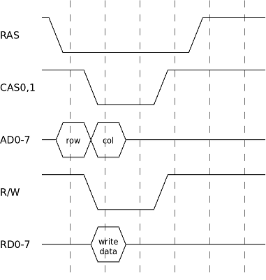
So a full write cycle takes 6 VDP clock cycles.
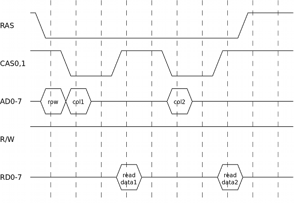
Reads are very similar to writes, they follow this schema:
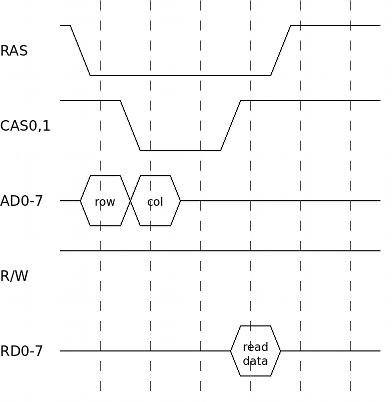
So this is very similar to a write: address selection is identical. Obviously the R/W signal and the direction (and timing) of the information on the data bus is different. And just like a write, a full read cycle also takes 6 VDP cycles.
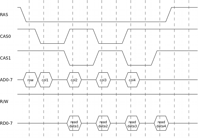
Often the VDP needs to read data from successive VRAM addresses. If those addresses all have the same row address, then there's a faster way to perform this compared to doing multiple reads like in the schema above.
The above diagram shows a burst-length of only two bytes. It's also possible to have longer lengths. The VDP uses lengths up-to 4 bytes (or 8, see next section).
In this example reading two bytes takes 10 VDP cycles. Doing two single reads would take 2×6=12 cycles. When doing longer bursts, the savings become bigger. Doing a burst of N reads takes 2+4×N cycles compared to 6×N cycles for a sequence of single reads.
In principle it's also possible to do burst-writes. Though the VDP doesn't use them (it never needs to write more than 1 byte in a sequence).
Burst reads are already faster than single-reads. But to be able to render screen 7 and 8 images, burst reads are still not fast enough. In these two screen modes, to be able to read the required data from VRAM fast enough, the VDP reads from two banks in parallel.
There are 2 banks of 64kB. These two banks share the RAS control signal, but they each have their own CAS signal. The address and data signals are also shared. This allows to read from both banks almost in parallel:
So this schema gives (almost) double the VRAM-bandwidth. The only requirement is that you alternatingly read from bank0 and bank1. At first sight this requirement seems so strict that it is almost never possible to make use of this banked reading mode: to render screen 7 or 8 you indeed need to read many successive VRAM locations, not locations that alternatingly come from the 1st and 2nd 64kB bank.
To make it possible to use banked reading mode, the VDP interleaves the two banks. This introduces the concept of logical and physical addresses:
In most screen modes the logical and the physical addresses are the same. But in screen 7 and 8 there's a transformation between the two:
physical = (logical >> 1) | (logical << 16)
So the 17-bit logical address is rotated one bit to the right to get the physical address. The effect of this transformation is that all even logical addresses end up in physical bank0 while all odd logical addresses end up in physical bank1. So now when you read from successive logical addresses you read from alternating physical banks and thus it is possible to use banked read mode.
Usually a VDP programmer doesn't need to be aware of this interleaving. But because interleaving is only enabled in screen 7 and 8, this effect can become visible when switching between screen modes. An alternative design decision could have been to always interleave the addresses. I guess the V9938 designers didn't make this choice to allow for single chip configurations in case only 64kB VRAM is connected.
The diagram above shows a read of 2×2 bytes, in reality the VDP only uses this schema to read 2×4 bytes. In principle it's also possible to write to two banks in parallel, but the VDP never needs this ability.
DRAM chips need to be refreshed regularly. The VDP is responsible for doing this (there are DRAM chips that handle refresh internally, but the VDP doesn't use such chips). Many DRAM chips allow a refresh by only activating and deactivating the RAS signal, so without actually performing a read or write in between. When extrapolating from the above timing diagrams, this would only cost 4 cycles. Though the VDP doesn't actually use this RAS-without-CAS refresh mode. Instead it performs a regular read access which takes 6 cycles.
Each time a read (or write) is performed on a certain row of a DRAM chip, that whole row is refreshed. So to refresh the whole RAM, the VDP has to periodically read (any column address of) each of the 256 possible rows.
The previous section described the details of isolated (single or burst) VRAM accesses. This section will look at such accesses as indivisible units and examine how these units are grouped together and spread in time to perform all the VRAM related stuff the VDP has to do.
The VDP can perform VRAM reads/writes for the following reasons:
Note that next to bitmap modes, the VDP also has character and text modes. I didn't investigate those modes yet, so this text mostly ignores them.
The rest of this text explains when in time (at which specific VDP cycles) accesses of each type are executed.
We'll first focus on refresh and bitmap/sprite rendering. Later we'll add CPU and command engine. The reason for this split is that the first group has a fairly simple pattern: refreshes always occur at fixed moments in time. Enabling bitmap rendering only adds additional VRAM reads but has no influence on the timing of the refreshes. Similarly enabling sprite rendering adds even more reads without influencing the bitmap or refresh reads. CPU and command accesses on the other hand cannot simply be added to this schema without influencing each other. So those are postponed till a later section.
The VDP renders a full frame line-by-line. For each line the VDP (possibly) has to read some bitmap and sprite data from VRAM. It's logical to assume (and the measurements confirm this) that the data fetches within one line occur at the same relative positions as the corresponding data fetches of another line. So if we can figure out the details for one line, we can extrapolate this to a whole frame. Similarly we can assume that different frames will have similar relative timings. So really all we need to know is the timing of one line.
TODO: odd and even frames in interlace mode probably do have timing differences. Still need to investigate this.
Let's thus first look at what we already know about an horizontal display line. The 'V9938 Technical Data Book' contains the following timing info about (non-text mode) display lines.
| Description | Cycles | Length |
|---|---|---|
| Synchronize signal | [0 - 100) | 100 |
| Left erase time | [100 - 202) | 102 |
| Left border | [202 - 258) | 56 |
| Display cycle | [258 - 1282) | 1024 |
| Right border | [1282 - 1341) | 59 |
| Right erase time | [1341 - 1368) | 27 |
| Total | [0 - 1368) | 1368 |
So one display line is divided in 6 periods. The total length of one line is 1368 cycles. The previous section showed how long individual VRAM accesses take. The next sections will figure out how all the required accesses fit in this per-line budget of 1368 cycles.
A note about the timing notation: in this text all the timing numbers are VDP cycles relative within one line. For example in the table above the display period starts at cycle 258. The display period of the next line will start at cycle 258+1368=1626, the next at cycle 2994 and so on. To make the values smaller, all cycle numbers will be folded to the interval [0, 1368). The staring point (cycle=0) has no special meaning. We could have taken any other point and called that the starting point. (For the current choice, the external VDP HSYNC pin gets activated at cycle=0, so it was a convenient point to synchronize the measurements on).
TODO horizontal set-adjust: The numbers in the above table are valid for horizontal set-adjust=0. Similarly all our measurements were done with set-adjust=0. Using different set-adjust values will make the left/right border bigger/smaller. I still need to figure out which timing values of the next sections are changed by this. E.g. are all the VRAM accesses in a line shifted as a whole, or are just the bitmap data fetches shifted and remain (some) other accesses fixed?
TODO bits S1,S0 in VDP register R#9: The above table is valid for S1,S0=0,0. In other cases the length of a display line is only 1365 cycles instead of 1368. The rest of this text assumes a line length of 1368 cycles. I still need to figure out where exactly in the line this difference of 3 cycles is located.
The following image graphically summarizes the results of the rest of this section. This is a very wide image, it is much larger than what can be shown inline in this text (click to see the full image). It's highly recommended to open this image in an external image viewer that allows to easily zoom in and out and scroll the image.
Here's an overview of the most important items in this image:
The next sections will go into a lot more detail. It's probably a good idea to have this (zoomed in) image open while reading those later sections.
When looking from a VDP-VRAM interaction point of view, the VDP can operate in 3 modes:
Note that the (bitmap) screen mode (screen 5, 6, 7, or 8) largely doesn't matter for the VRAM access pattern.
TODO sprite fetching happens 1 line earlier than displaying those sprites (see below for details). This means that the last line of the vertical border before the display area likely uses a 'mixed mode' where it doesn't yet fetch bitmap data but it does already fetch sprite data. I didn't specifically measure this condition, so I can't really tell anything about this mixed mode. (One possibility is that it's just like a normal display line, but the fetched bitmap data is ignored.) Similarly the last line of the display area doesn't strictly need to fetch new sprite data.
We'll now look at these 3 modes in more detail.
Screen rendering can be disabled via bit 6 in VDP register R#1. There's also no screen rendering when the VDP is showing a vertical border line. From a VRAM-access point of view both cases are identical.
In this mode the VDP doesn't need to fetch any data from VRAM for rendering. It only needs to refresh the VRAM. As already mentioned earlier, the VDP uses a regular read to refresh the RAM, so this takes 6 cycles.
The VDP executes 8 refresh actions per display line. They start at the following moments in time (the red blocks in the big timing diagram):
| 284 | 412 | 540 | 668 | 796 | 924 | 1052 | 1180 |
I didn't investigate this refresh-address-stuff in detail because it doesn't matter for emulation accuracy.
The logical addresses used for refresh reads seems to be of the form:
N×0x10101 | 0x3F
Where N increases on each refresh action. So each refresh the row address increases by one and every other refresh either the CAS0 or the CAS1 signal gets used (the columns address doesn't matter for refresh). Note that this formula is for the logical address, in screen 7/8 this still gets transformed to a physical address. So in screen 7/8 a refresh action always uses the CAS1 signal. That means that in screen 7/8 the DRAM chip(s) of bank0 actually do get refreshed using the RAS-without-CAS refresh mode.
The refresh timings are the same for all non-text screen modes. But in text modes there are only 7 refreshes per line and they are also located at different relative positions than in the table above. I didn't investigate this further.
Next to the refresh reads, in 'screen disabled' mode, the VDP still performs 4 reads of address 0x1FFFF. At the following moments (marked with dark-grey blocks on the timeline):
| 1236 | 1244 | 1252 | 1260 |
I can't image any use for these reads, so let's call them dummy reads. In all our measurements these dummy reads always re-occur in these same positions, so it's not a fluke in (only one of) the measurements.
The refresh actions remain exactly the same in the other two modes. But these dummy reads are different in the mode 'sprites off' or disappear completely in the mode 'sprites on'. (This confirms that nothing 'useful' is done by these dummy reads).
Anyway for emulation we can mostly ignore these dummy reads. It only matters that at these moments in time there cannot be CPU or command VRAM reads or writes.
Refresh works exactly the same as in the previous mode. The dummy reads are a bit different. Now there are only 3 dummy reads at slightly different moments (also shown in dark-grey):
| 1242 | 1250 | 1258 |
The first of these 3 reads is always from address 0x1FFFF. The second and third dummy read have a pattern in their address. For example:
| 1st | 2nd | 3rd |
|---|---|---|
| 0x1FFFF | 0x03B80 | 0x03B82 |
| 0x1FFFF | 0x03C00 | 0x03C02 |
| 0x1FFFF | 0x03C80 | 0x03C82 |
| 0x1FFFF | 0x03D00 | 0x03D02 |
This table shows the addresses of the 3 dummy reads for 4 successive display lines (this is data from an actual measurement, unfortunately our equipment could only buffer up to 4 lines). The lower 7 bits of the address of the 2nd read always seem to be zero. The address of the 3rd read is the same as for the 2nd read except that bit 1 is set to 1. When going from one line to the next, the address increases by 0x80. Our measurements captured 10 independent sets of 4 successive lines. Each time bits 16-15 were zero (bits 14-7 do take different values). This could be a coincidence, or it could be that these bits really aren't included in the counter. Note that again these are logical addresses (so still transformed for screen 7/8). I didn't investigate these dummy reads in more detail because they mostly don't matter for emulation.
The major change compared to the previous mode is that now the VDP needs to fetch extra data for the bitmap rendering. These fetches happen in 32 blocks of 4 bytes (screen 5/6) or 8 bytes (screen 7/8). The fetches within one block happen in burst mode. This means that one block takes 18 cycles (screen 5/6) or 20 cycles (screen 7/8). Though later we'll see that the two spare cycles for screen 5/6 are not used for anything else, so for simplicity we can say that in all bitmap modes a bitmap-fetch-block takes 20 cycles. This is even clearer if you look at the RAS signal: this signal follows the exact same pattern in all (bitmap) screen modes, so in screen 5/6 it remains active for two cycles longer than strictly necessary.
Actually before these 32 blocks there's one extra dummy block. This block has the same timing as the other blocks, but it always reads address 0x1FFFF. From an emulator point of view, these dummy reads don't matter, it only matters that at those moments no other VRAM accesses can occur.
The start of these 1+32 blocks are located at these moments in time (these are the green blocks in the big timing diagram):
| (195) | 227 | 259 | 291 | 323 | 355 | 387 | 419 | 451 |
| 483 | 515 | 547 | 579 | 611 | 643 | 675 | 707 | |
| 739 | 771 | 803 | 835 | 867 | 899 | 931 | 963 | |
| 995 | 1027 | 1059 | 1091 | 1123 | 1155 | 1187 | 1219 |
The following is only speculation: I wonder why there is such a dummy preamble block. Theoretically this could have been used (or reserved) to implement V9958-like horizontal scrolling without having to mask 8 border pixels. Unfortunately horizontal scrolling on a V9958 doesn't work like that :(
Refresh and bitmap reads are exactly the same as in the previous mode. But the 3 or 4 dummy reads from the previous 2 modes are not present in this mode.
I've only investigated bitmap modes, that means the stuff below applies only to sprite mode 2.
For sprite rendering you need to:
Figuring out which sprites are visible is done by reading the y-coordinates of each of the 32 possible sprites. These reads happen interleaved between the 32 block-reads of the bitmap data, so read one byte between each bitmap-block. Because of this interleaving it's not possible to use burst mode, so each read takes 6 cycles. There's also 1 dummy read of address 0x1FFFF at the end. The reads happen at these moments in time (yellow blocks between the green blocks in the diagram):
| 182 | 214 | 246 | 278 | 310 | 342 | 374 | 406 | |
| 438 | 470 | 502 | 534 | 566 | 598 | 630 | 662 | |
| 694 | 726 | 758 | 790 | 822 | 854 | 886 | 918 | |
| 950 | 982 | 1014 | 1046 | 1078 | 1110 | 1142 | 1174 | (1206) |
In the worst case, the 8 last sprites of the attribute table are visible. In that case all 32 reads are really required. Though even if the limit of 8 visible sprites is reached earlier, the VDP continues fetching all 32+1 bytes. Also if one y-coordinate is equal to 216 (meaning that all later sprites are invisible), still all 32+1 fetches are executed.
Once the VDP has figured out which sprites are visible it needs to fetch the data to actually draw the sprites. This VRAM access pattern is relatively complex:
| 1238 | 1251 | 1270 | 1280 | 1286 | 1296 |
| 1302 | 1315 | 1338 | 1348 | 1354 | 1364 |
| 2 | 15 | 34 | 44 | 50 | 60 |
| 66 | 79 | 98 | 108 | 114 | 124 |
It's worth repeating that whenever sprites are enabled, the VDP always performs the same fetch-pattern. So even if no sprites are actually visible, or if sprites are partially disabled (with y=216), and even with 8x8 vs 16x16 sprites, magnified or not. This confirms the fact that the VDP command engine is slowed down by the exact same amount in all these situation. Also all (bitmap) screen modes behave exactly the same with respect to sprite data fetches.
The previous sections explained when the VDP reads from VRAM for refresh and bitmap/sprite rendering (and even some dummy reads). Depending on the mode (screen/sprites enabled/disabled), this takes more or less of the available VRAM-bandwidth. The portion of the VRAM bandwidth that is not used for rendering can be used for CPU or command engine VRAM reads or writes.
All CPU and command engine accesses are single (non-burst) accesses, so they take 6 cycles each. However it is not the case that whenever the VRAM bus is idle for 6 cycles, it can be used for CPU or command engine accesses.
Instead there are fixed moments in time where there could possibly start a cpu or command access, let's call these moments access slots. Each slot can be used for either CPU or command accesses (there are no slots that are uniquely reserved for either CPU or for commands). The position and the amount of access slots only depends on the VDP mode (screen off, sprites off, sprites on), not for example on the amount of actually visible sprites or on the (bitmap) screen mode.
The 3 tables below show the amount and the positions of the possible access slots for the 3 different modes (in the timing diagram these are the blue blocks):
| 0 | 8 | 16 | 24 | 32 | 40 | 48 | 56 | 64 | 72 |
| 80 | 88 | 96 | 104 | 112 | 120 | 164 | 172 | 180 | 188 |
| 196 | 204 | 212 | 220 | 228 | 236 | 244 | 252 | 260 | 268 |
| 276 | 292 | 300 | 308 | 316 | 324 | 332 | 340 | 348 | 356 |
| 364 | 372 | 380 | 388 | 396 | 404 | 420 | 428 | 436 | 444 |
| 452 | 460 | 468 | 476 | 484 | 492 | 500 | 508 | 516 | 524 |
| 532 | 548 | 556 | 564 | 572 | 580 | 588 | 596 | 604 | 612 |
| 620 | 628 | 636 | 644 | 652 | 660 | 676 | 684 | 692 | 700 |
| 708 | 716 | 724 | 732 | 740 | 748 | 756 | 764 | 772 | 780 |
| 788 | 804 | 812 | 820 | 828 | 836 | 844 | 852 | 860 | 868 |
| 876 | 884 | 892 | 900 | 908 | 916 | 932 | 940 | 948 | 956 |
| 964 | 972 | 980 | 988 | 996 | 1004 | 1012 | 1020 | 1028 | 1036 |
| 1044 | 1060 | 1068 | 1076 | 1084 | 1092 | 1100 | 1108 | 1116 | 1124 |
| 1132 | 1140 | 1148 | 1156 | 1164 | 1172 | 1188 | 1196 | 1204 | 1212 |
| 1220 | 1228 | 1268 | 1276 | 1284 | 1292 | 1300 | 1308 | 1316 | 1324 |
| 1334 | 1344 | 1352 | 1360 |
| 6 | 14 | 22 | 30 | 38 | 46 | 54 | 62 | 70 | 78 |
| 86 | 94 | 102 | 110 | 118 | 162 | 170 | 182 | 188 | 214 |
| 220 | 246 | 252 | 278 | 310 | 316 | 342 | 348 | 374 | 380 |
| 406 | 438 | 444 | 470 | 476 | 502 | 508 | 534 | 566 | 572 |
| 598 | 604 | 630 | 636 | 662 | 694 | 700 | 726 | 732 | 758 |
| 764 | 790 | 822 | 828 | 854 | 860 | 886 | 892 | 918 | 950 |
| 956 | 982 | 988 | 1014 | 1020 | 1046 | 1078 | 1084 | 1110 | 1116 |
| 1142 | 1148 | 1174 | 1206 | 1212 | 1266 | 1274 | 1282 | 1290 | 1298 |
| 1306 | 1314 | 1322 | 1332 | 1342 | 1350 | 1358 | 1366 |
| 28 | 92 | 162 | 170 | 188 | 220 | 252 | 316 | 348 | 380 |
| 444 | 476 | 508 | 572 | 604 | 636 | 700 | 732 | 764 | 828 |
| 860 | 892 | 956 | 988 | 1020 | 1084 | 1116 | 1148 | 1212 | 1264 |
| 1330 |
Note that even in the mode 'screen off', when the VRAM bus is otherwise mostly idle, the access slots are still at least 8 cycles apart. A single access takes only 6 cycles, so 2 cycles are wasted.
Very roughly speaking in mode 'screen off' there are about twice as many access slots as in the mode 'sprites off' and about 5 times as many as in the mode 'sprites on'. This does however not mean that in these modes the command engine will execute respectively 2× and 5× as fast. Instead in the mode 'sprites on' the speed of command execution is mostly limited by the amount of available access slots, while in the mode 'screen off', the bottleneck is mostly the speed of the command engine itself.
Also note that the access slots are not evenly spread in time. For example:
These large gaps between the access slots are important. For example if the CPU is sending data to the VDP at a too fast rate, and this happens right at a moment where there are no access slots available, then some of the data send by the CPU is lost. We'll see later in this text that this can even happen when the time between the incoming CPU requests is (slightly) larger than the size of the largest gap.
The access slots can be used for either CPU or VDP command reads or writes. This section explains how the slots are allocated to these two subsystems.
The basic principle is very simple: the CPU or the command engine take the first available access slot. And when the CPU and command engine both require an access slot at the same time, then the CPU gets priority. Though if you look at the details it is a bit more complicated:
A surprising result (at least to me) of these measurements is that the speed of VDP command execution is reduced while simultaneously doing CPU VRAM accesses. Looking back this makes sense because the same VRAM access slots are shared between CPU and command engine and the CPU gets priority.
This effect is clearly noticeable in the mode 'sprites on' but much less in the other two modes. This is easily explained by looking at the amount of available access slots in these modes.
The most extreme situation occurs in this test. Execute a HMMV VDP command
(this is the fastest command, see below) while simultaneously executing a long
series of OUT (#98),A instructions (the fastest way to send CPU
write requests). In our measurements, in the mode 'sprites on' the command
execution speed was approximately cut in half! But in the other two modes, the
execution speed was barely influenced. (Actually our test program wasn't
accurate enough to measure any significant speed difference, but theoretically
also in the latter two modes the execution speed should be reduced by a small
amount).
The fastest way for the Z80 to send read or write VRAM request to the VDP is
by using a sequence of IN A,(#98) or OUT (#98),A
instructions (of course such a sequence always writes the same value or ignores
all but the last read value). This takes 12 Z80 clock cycles per request.
(Instructions like OUT (C),r or OUTI are all slower).
The VDP is clocked at 6× the Z80 speed. So when the Z80 sends multiple
requests to the VDP, the minimal distance between these requests, translated to
VDP cycles, is at least 72 VDP cycles. Earlier we saw that the maximal gap
between access slots was 70 VDP cycles, so at first sight there's no problem.
However consider this scenario:
OUT (#98),A
instruction) after the previous request. But the buffer still contains the
previous unhandled request. The new request overwrites the old request!Note that this scenario used a gap of only 64 VDP cycles between access slots, while there were 72 cycles between the CPU requests. (And the largest gap between access slots is 70 cycles).
The command engine needs access to VRAM. In the previous section we saw when the VDP will grand access to this subsystem: when there's an access slot available and when that slot is not already allocated to CPU access. In this section we'll see when exactly the command engine will generate VRAM access requests. Obviously the type (read or write) and the rate of these requests depends on the type of the VDP command that is executing.
Some commands (like HMMV) only need to write to VRAM. Other commands (like LMMM) need 2 reads and 1 write per pixel. Many commands execute on a block (a rectangle) of pixels. Such a block is executed line per line (all pixels within one horizontal line are processed before moving to the next line). Moving from one line to the next takes some amount of time (but YMMM is an exception, see below). This means that e.g. a HMMM command on a 20x4 rectangle executes faster than on a 4x20 rectangle (same amount of pixels in both cases, but a different rectangle shape).
The following table summarizes the timing for all measured commands:
| Command | Per pixel | Per line |
|---|---|---|
| HMMV | 48 W | 56 |
| YMMM | 40 R 24 W | 0 |
| HMMM | 64 R 24 W | 64 |
| LMMV | 72 R 24 W | 64 |
| LMMM | 64 R 32 R 24 W | 64 |
| LINE | 88 R 24 W | 32 |
TODO timing for PSET, POINT, SRCH
I'll explain the notation in this table with an example. Take the LMMM command:
All the commands in the table above are block commands except for 'LINE'. For the LINE command the meaning of the columns 'Per pixel' and 'Per line' may not be immediately clear:
Note that for the YMMM command there's no extra overhead when going from one horizontal line to the next. This might be related to the fact that a line of a YMMV command always starts at the left or right border of the screen.
TODO What we didn't measure (also couldn't measure with our test setup) was the delay between the start of the command (when the CPU sends the command byte to the VDP) and the moment the command actually starts executing (e.g. when the first read or write command access is send to VRAM). It's logical to assume that the 'per line' overhead also occurs at the start of the command. But it's possible there is also some additional 'per command' overhead.
When looking at the above table, we see that the command engine is very slow. For example in a HMMM command there are 24 cycles between reading a byte and writing that byte to the new location. Or in a LINE command it takes 32 cycles to take a step in the minor direction. I believe there are two main reasons for this slowness:
Taking these two points into account, the above table can be rewritten as:
| Command | Per pixel | Per line |
|---|---|---|
| HMMV | (4×8+16) W | 7×8 |
| YMMM | (3×8+16) R (1×8+16) W | 0×8 |
| HMMM | (6×8+16) R (1×8+16) W | 8×8 |
| LMMV | (7×8+16) R (1×8+16) W | 8×8 |
| LMMM | (6×8+16) R (2×8+16) R (1×8+16) W | 8×8 |
| LINE | (9×8+16) R (1×8+16) W | 4×8 |
When you look at the data in this way, the numbers already look more reasonable.
All the information above should already be enough to significantly improve the accuracy of MSX emulators. The following months I plan to work on improving openMSX.
I'm afraid this will all still take quite a bit of work.
Anyway, I hope the information in this document is useful. For (other) MSX emulator developers or for MSX developers in general.
2013/03/30, Wouter Vermaelen