This text is a follow-up on the earlier V9938 VRAM timings document. If you haven't done so already it's probably a very good idea to (re-)read that document first, because this text assumes you remember all the earlier details ;-)
Early 2013 the openMSX team made some logic-analyzer-measurements of the actual communication between a V9938 and the connected VRAM. The goal of those measurements was to improve the emulation of the VDP command engine in openMSX. That goal was fully achieved: to the best of our knowledge the timing of the VDP command engine is now fully accurate: e.g. recent versions of openMSX now generate identical pictures as real MSX machines for the LINE-speed test picture shown in the motivation section of the previous document.
A nice side effect of these measurements was that, next to the command engine speed, we also obtained information about what happens when the CPU (Z80) reads or writes the VRAM too fast, and what exactly is "too fast". This behaviour is now also implemented in openMSX, though only (yet) for the V9938 bitmap screen modes (the information in this text should allow us to also implement the timing for the other screen modes).
Because the focus was the command engine and because a V9938 can only execute commands in bitmap screen modes (screen 5-8), our measurements were mostly focused on those screen modes. And especially the analysis of the results was initially focused on the bitmap screen modes. In this text we will now look at the other screen modes, even though there is less measurement data available for those modes.
The second half of this text looks at the TMS9918 VDP. We only made measurements on a V9938 and as we'll see below the results cannot be extrapolated to TMS9918. Luckily there are other sources of information available that allow to piece together similar (though less detailed) timing diagrams for the TMS9918 as for the V9938.
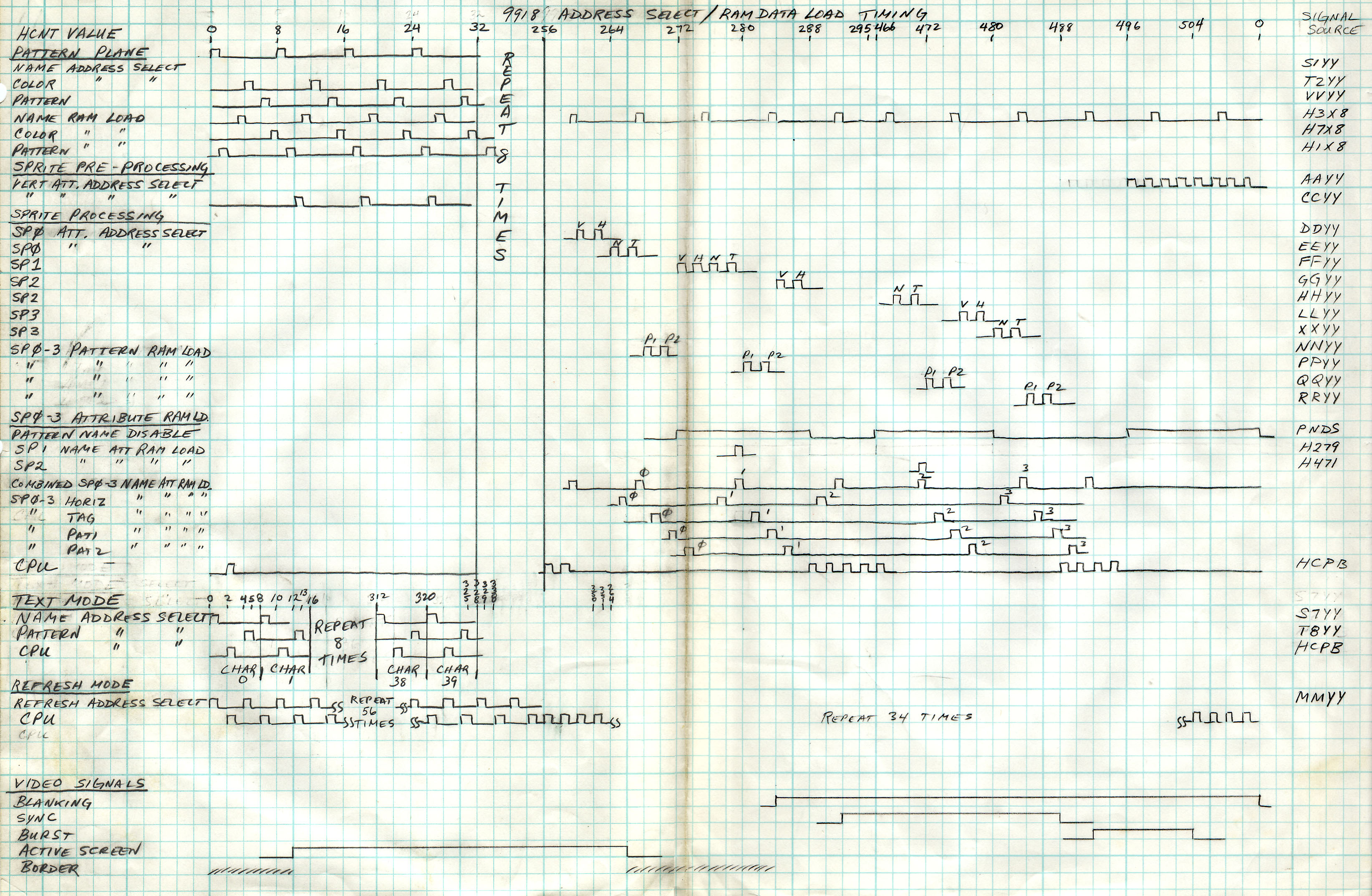
Similar like in the previous document, we'll start by presenting all the results in one big diagram. I strongly recommend to open this image in an image viewer that easily allows to scroll and zoom-in and -out (so maybe not a web-browser). It may also be useful to have this image open while reading the later sections in this text.

At the top of this diagram the results of the previous article are repeated, these are the V9938 bitmap modes. In the middle are the V9938 character- and text-modes. And at the bottom you see the TMS9918 results. They're all included in one big diagram to allow to more easily compare them.
Horizontally you see the detailed timing of one display line. On V9938 one line takes 1368 cycles, on TMS9918 it takes 342 cycles. The line is divided in different phases (indicated by the different background colors) corresponding to the left- and right-border, display cycle, etc. Notice that the text modes have different border widths than the other modes. Also notice that the lengths of these periods are not exactly the same between the two VDP types.
Because these horizontal phases don't fully correspond between the two VDP types, I had to make a choice in how to align the results of both VDPs. I choose to align the display cycle (the period where the actual pixels are shown). Though this means that 'cycle 0' is not located in exactly the same horizontal position for both VDPs. But this doesn't matter: as explained in the previous article, 'cycle 0' is anyway an arbitrary choice. Just keep it in mind when comparing the results.
For the V9938 the diagram shows the RAS and CAS0/1 signals, for TMS9918 that information is missing. But that's OK: on V9938 there are burst and non-burst accesses, there are idle cycles, dummy accesses, etc. So the RAS/CAS signals do provide extra information. As we'll see in the 2nd half of this text, on TMS9918 the communication with the VRAM is much simpler, so the RAS/CAS signals anyway don't contribute as much extra information.
In this section we'll look at the 3 character-based display modes: Graphics Mode 1, Graphics Mode 2 and Multi-color Mode (aka screen 1, 2 and 3). As we'll see, from a VRAM access point of view, these 3 modes are closely related.
The VRAM needs to be regularly refreshed. The V9938 does this by regular reads (from all banks of the DRAM chips). Those reads are located at the following moments in time (VDP cycle counts within one display line). Remember that one display line has 1368 VDP cycles and that cycle 0 is semi-arbitrarily chosen within the line (so only relative numbers matter).
| 284 | 412 | 540 | 668 | 796 | 924 | 1052 | 1180 |
Note that these are the exact same locations as for the bitmap screen modes.
To be able to render each character we need to:
There are 32 characters on a line, so these 3 reads also repeat 32 times. The name-, pattern- and color-table reads are located at these respective moments in time:
| 214 + 32n + 0 | 214 + 32n + 18 | 214 + 32n + 24 | with 0 ≤ n < 32 |
Notice there's some room between the name-table read and the pattern-/color-table reads. The address required to read from the latter two tables depends on the result obtained from the first read. So possibly there's extra room at this location to give the VDP more time to calculate those addresses. In fact there fit exactly 2×6 cycles between the name- and pattern-table read. This leaves room for 2 other VRAM accesses:
Above we saw there are 32 reads to figure out which sprites are visible. In this section we'll see what additional VRAM reads are performed to actually render the visible sprites.
In sprite mode 1 there are maximally 4 sprites visible on a line. For each of those we need to read the sprite attributes (this is the x- and y-coordinate, the sprite pattern number and the sprite color). And we also need to read 1 or 2 bytes from the sprite-pattern-table (for 8×8 or 16×16 sprites). Similar to sprite mode 2, the y-coordinate is re-read (the sprite-visibility pass already read it). The VDP always reads 2 sprite pattern bytes (for 8×8 sprites that 2nd byte is ignored). And even if fewer than 4 sprites are actually visible, the VDP always performs VRAM reads for all 4 sprites (and ignores the results of the redundant reads).
| x+0 | x+4 | x+8 | x+12 | with x = 1242, 1306, 6, 70 |
| x+0 | x+4 | with x = 1274, 1342, 38, 102 |
Next there are a bunch of dummy reads:
(As you may have guessed already) all these dummy reads can be explained by looking at how the V9938 implements sprite mode 2:
(*)Actually, this is not true. But I believe this is how it was intended: the 6 bytes are located in the same DRAM bank. In reality the V9938 performs 2 burst reads of 3 bytes each. But because there are only 28 cycles available it has to use a, strictly speaking, invalid DRAM timing. See previous article for more details.
So the timing of all sprite mode 2 reads is (almost) identical to all the sprite mode 1 normal + dummy reads, only slightly shifted in time.
I guess all these dummy reads in sprite mode 1 are the result of chip-area optimizations done by Yamaha engineers. In the current design the same state machine can generate the CAS/RAS signals for both sprite modes. And similarly a large part of the address generation logic for sprite mode 1 and 2 can be shared. But unfortunately it does mean the VRAM bandwidth used for those dummy reads is not available for CPU VRAM access or (on V9958) for command execution.
Next to all the dummy reads related to sprite rendering, there are also dummy reads at these moments in time:
| 182 | 200 | 206 | 1218 |
These are the locations where you would expect respectively reads from the name-, pattern-, color-, and sprite-attribute-table if you'd extend a display line to 33 instead of 32 characters. This is similar to how in the bitmap screen modes there is a dummy preamble for the bitmap data and a dummy postamble for the sprite y-coordinate. All 4 dummy reads read address 0x1ffff.
These are the available CPU/cmd access slots:
| 32 | 96 | 166 | 174 | 188 | 220 | 252 | 316 | 348 | 380 |
| 444 | 476 | 508 | 572 | 604 | 636 | 700 | 732 | 764 | 828 |
| 860 | 892 | 956 | 988 | 1020 | 1084 | 1116 | 1148 | 1212 | 1268 |
| 1334 |
This is very similar to the CPU/cmd slots in bitmap mode with sprites enabled. In both cases there are 31 available slots and the largest distance between (the start of) two slots is 70 VDP cycles. Only some of the slots are slightly shifted when comparing both modes.
From a VRAM access point of view this mode is quasi identical to Graphics mode 2. It does exactly the same number of VRAM reads as Graphics mode 2 at exactly the same moments in time. Only the addresses in the color-table are a bit different. So it does re-read the same color information for all 8 lines in a character.
Maybe surprisingly, from a VRAM access point of view, also this mode is quasi identical to Graphics mode 2. This mode doesn't have a color-table. But the V9938 still uses the same VRAM access schema as it uses for Graphics mode 2. The reads from the color-table are replaced with dummy reads from address 0x1ffff, but all the rest is identical.
So unfortunately the VRAM bandwidth used to access the color-table does not become available for CPU-VRAM access (or the command engine on V9958).
Now we'll look at the two text modes. We'll again see that, from a VRAM access point of view, both modes are very similar.
In all V9938 bitmap and character modes the refresh was handled identically. For text modes it's different. Now there are only 7 (instead of 8) refresh reads per display line and they are clustered together near the start of the line, located at these moments in time:
| 74 | 82 | 90 | 98 | 106 | 114 | 122 |
So apparently 7 refreshes per line are enough to keep the DRAM content intact. Too bad the other screen modes use 8. Also using only 7 could have made command execution slightly faster.
There are 2 dummy reads from address 0x1ffff located at:
| 230 | 238 |
| g+0 | g+4 | g+8 | g+12 |
with g one of:
| 246 | 294 | 342 | 390 | 438 | 486 | 534 | 582 | 630 | 678 |
| 726 | 774 | 822 | 870 | 918 | 966 | 1014 | 1062 | 1110 | 1158 |
Next we read 1 byte from the color-table (at cycle g+18). This gives 8 bits, so we only need to do this for every other group (in the other group this access is used as a CPU/cmd access slot). Last we read 4 bytes from the pattern table. These must be non-burst reads because potentially bits 15-8 of the pattern-address for each character are different. These reads start at:
| g+24 | g+30 | g+36 | g+42 |
Note that combined all reads in 1 group take 48 cycles, and that's also the distance between 2 groups (in character mode there where a few spare cycles in a group). So it is really required to process the characters in groups of 4, otherwise burst reads aren't possible and all the required VRAM accesses don't fit in the available cycle budget (1 narrow pixel is 2 VDP cycles, thus 4 characters of each 6 pixels take 48 cycles).
These are the positions of the available CPU/cmd access slots:
| 2 | 10 | 18 | 26 | 34 | 42 | 50 | 58 | 66 | 166 |
| 174 | 182 | 190 | 198 | 206 | 214 | 222 | 312 | 408 | 504 |
| 600 | 696 | 792 | 888 | 984 | 1080 | 1176 | 1206 | 1214 | 1222 |
| 1230 | 1238 | 1246 | 1254 | 1262 | 1270 | 1278 | 1286 | 1294 | 1302 |
| 1310 | 1318 | 1326 | 1336 | 1346 | 1354 | 1362 |
There are 47 access slots, but they are very unevenly distributed. Often the distance between two slots is 96 cycles, and one time even 100 VDP cycles! This means that, even though there are more slots compared to bitmap/character mode, the Z80 must access the VRAM more slowly in this mode! So to be safe there must be 20 Z80 cycles between two CPU-VRAM accesses (see previous article for the details of this calculation).
As mentioned before, from a VRAM access point of view, Text mode 1 is similar to Text mode 2. Actually from a VRAM access allocation point of view it's identical, only the actually VRAM read addresses are different. This may seem strange because Text mode 1 logically needs a lot less data than Text mode 2. This is because over half of the performed reads are dummy reads:
The available CPU/cmd access slots are identical to those in Text mode 2. It's unfortunate there are so many dummy reads in this mode. If this wasn't the case, the available VRAM bandwidth for CPU accesses (or commands on V9958) could have been a lot higher. Especially because the Z80 already cannot access VRAM very fast in this mode. And also because, as we'll see below, on TMS9918 there's no such timing constraint for this mode.
There are a number of V9938 cases we don't have measurements for. As already said in the beginning of this text, the original goal of these measurements was to improve the accuracy of the command engine emulation. And we only had a very limited amount of time the day we did this experiment. Re-doing the experiment is certainly possible and not even that hard. But it takes a lot of time to setup, for, as we'll see below, not too much useful extra knowledge. But of course I'd be very happy to hear from other people who do want to repeat and/or extend our measurements!
This uses very likely the same timing as Graphics mode 2 (aka screen 2), but with the address generation logic of sprite mode 1 replaced with the one for sprite mode 2. The timing of all VRAM accesses, even the sprite accesses, can remain identical. The existence of this screen mode might have been (another) reason to design the timing of sprite mode 1 on V9938 in such a strange way.
In bitmap modes, when sprite rendering is disabled, the VRAM bandwidth that was allocated to sprite rendering becomes available for CPU/cmd accesses. Likely the same is true for character modes (and text modes never have sprites). Unfortunately since we didn't measure this combination we don't know exactly where those slots are located. But it should be possible to make a very reasonable estimate.
All non-text modes behave identical when screen display is disabled (and the behavior during screen disabled is identical to the behavior during vertical border lines): the VRAM reads for screen- and sprite-rendering are gone and replaced by CPU/cmd access slots, but e.g. the refresh accesses remain. In the 2 text modes those refresh accesses are located in different positions compared to bitmap/character modes. It's not known whether:
This might make a difference for the exact position of the CPU/cmd access slots. But because there are usually plenty of slots available in screen-off mode, this likely won't matter (much).
All our measurements were performed on a V9938 (MSX2 VDP). It's very likely we can extrapolate the results to a V9958 (MSX2+ VDP). But for sure we cannot use these results to derive anything meaningful for the TMS9918. Fortunately there already is some interesting information available in these documents from Karl Guttag. Especially this timing picture looks promising. Combined with information found in the TMS9918 application manual I was able to deduce the stuff below. This wasn't easy because that timing picture does contain some (confusing) mistakes, although I can easily forgive those mistakes because drawing this stuff by hand is very tedious ;-)
The TMS9918 runs at 5.37MHz (1.5×3.58MHz, 4× slower than the V9938). One display line takes 342 cycles (as expected, 4× less than on V9938). One memory access takes only 2 cycles or 372ns. So compared to V9938 each memory access takes slightly longer (on V9938 one access takes 6 cycles or 279ns). The TMS9918 never uses burst memory reads.
For the actual arrangement of the accesses I'll refer to the big timing diagram (see top of this article). Most things are reasonably straight-forward. One notable thing is the arrangement of the 32 sprite y-coordinate reads (for the visibility check): the first 8 follow a different pattern than the last 24. This is done to not have too long periods without CPU VRAM access slot. Reading the other sprite data (during the horizontal border) also shows some irregularities. Like on V9938, the y-coordinates of the visible sprites are read twice, but apart from these 4 redundant reads, there are no dummy reads or idle cycles (unlike V9938). It is not known whether the TMS9918 performs reads for sprites that are not actually visible or that those slots are available for CPU access (V9938 performs dummy reads).
The TMS9918 application manual mentions in section 2.1.5 "… CPU windows occur once every 16 memory cycles …". This confirms the above.
I couldn't find anything specific about the timing of this mode in the above documentation. But because it requires the same number of reads from VRAM as Graphics mode 2, it's logical to assume the timing is identical.
The documentation also doesn't have specific timing information for this mode. In this mode the color-table isn't used, so one possibility is that accesses to the color-table are replaced by CPU access slots (not the case on V9938). This is confirmed by the following quote from the application manual, section 2.1.5 "… in the Multicolor mode, CPU windows occur at least once out of every four memory cycles …". Though when you look at the sprite-accesses in the horizontal border area this quote isn't true: there's still one location where there are 15 memory cycles between 2 CPU access slots! On the other hand, it would be possible to distribute the sprite and cpu accesses more evenly in the horizontal border. So maybe that hand-drawn timing picture is wrong? Or maybe it doesn't correspond to the final TMS9918 design?
Again see the big timing diagram. There's nothing really special about this mode. The following quote from the application manual confirms this arrangement: section 2.1.5 "… In the Text mode the CPU windows occur at least once out of every three memory cycles …". Note that reads from the name-table are not immediately followed by reads from the pattern-table. Possibly because the addresses in the latter table depend on the results from the former reads and the VDP needs time to calculate those addresses.
On TMS9918 there's no register that allows to disable sprite rendering (there is on V9938), but it is possible to disable the whole screen rendering. The documentation does hint that the screen-disabled behavior is the same as the behavior during the vertical border (just as on V9938).
You may have noticed that in the above TMS9918 display-mode sections we didn't mention any refresh reads. Also note that the hand-drawn TMS9918 timing picture mentions something called 'refresh mode' (but nothing called 'vertical border' or 'screen-disabled'). So I believe that on TMS9918 the VRAM is not refreshed during each display line, but instead it's refreshed during the vertical border.
On V9938 each display line performs 8 refresh reads (only 7 in text mode), so it takes 64 lines or about 4ms to refresh 128kB VRAM (and only 2ms if you rely on RAS-without-CAS refresh). On TMS9918 each vertical border line performs 32 refresh reads. So during the whole vertical border the full 16kB VRAM is fully refreshed multiple times. Though between two vertical borders there are 192 display lines or about 12ms. So DRAM chips connected to TMS9918 have to be able to retain their content longer without refresh than those connected to V9938. The TMS9918 refresh schema does make more efficient use of the available VRAM bandwidth (only do refresh when there's plenty of bandwidth available). On the other hand the TMS9918 schema would make something like the V9938-overscan-trick impossible (overscan = show display lines everywhere, 'skip' the vertical border).
So what do the above timings mean for a MSX1 Z80 programmer? In various fora (MSX or other) you find discussions about how fast it's allowed to access the VRAM (read/write data from/to IO port 0x98). The general consensus seems to be "at least 29 Z80 cycles between two accesses". For example an OUT(#99),A instruction takes 12 cycles (on MSX), so you need 17 extra cycles before the next such instruction.
This value of 29 cycles seems to come directly from the TMS9918 application manual: it says in the worst case there must be 6µs+2µs=8µs between two accesses. Translated to Z80 cycles this gives 28.6 and rounded up 29 Z80 cycles. Though IMHO this result isn't very satisfactory. That value 8µs is only given with one significant digit, so it could just as well be 7.5µs or 8.5µs. Rounded up to the nearest Z80 cycle that's between 27 and 31 Z80 cycles. Many people use the 29-cycles rule and apparently that works fine in practice. But you also see reports that only 28 cycles often(?)/always(?) work as well. It would be nice if we could measure the exact value.
That value 2µs is also mentioned in table 2.2 of the TMS9918 application manual. Other values in that table seem to be accurate to ±0.05µs, so it's possible (even likely?) those 2µs can be read as 2.0µs. It must be an integer multiple of VDP clock cycles: 10 cycles is 1.86µs, 11 cycles is 2.05µs. If I have to make a guess I'd pick the latter (this still results in a total CPU-VRAM access time of 29 Z80 cycles). Though in the rest of this text I'm still assuming the larger uncertainty interval.
Sometimes you find discussions about when it's allowed to go faster than the worst case requirement. Here the consensus is that in the vertical border you can go as fast as you want (seems to be correct, see below). Sometimes you see suggestions that it's also fine to go faster in the horizontal border or when sprites aren't used (this seems wrong, or at least only partly correct).
Anyway, in the remainder as this section I'd like to dig a little deeper. Now that the exact VRAM access allocation schemas are known we can say a little more. But unfortunately some details will remain unclear.
In the worst case (Graphics mode 1 and 2) there are 16 memory cycles (32 VDP cycles, 21.3 Z80 cycles) between two CPU slots. The application manual also mentions an additional CPU-access waiting time of 2µs. Though as explained above that could be anywhere from 1.5µs to 2.5µs, this is between 8 to 13 VDP cycles or 5 to 9 Z80 cycles. (It's not clear where this time is coming from, maybe something similar to the V9938 'slot-reservation' delay of 16 cycles). Combined this gives between 26.7 and 30.2 Z80 cycles. But unfortunately this isn't more accurate than the range we already found above.
In this post dvik suggests it's OK to use tighter timings when "sprites aren't used". This would mean that the memory slots that are otherwise used for sprite rendering are given to the CPU. But what does that mean "sprites aren't used"? If it means there simply aren't any sprites visible, the TMS9918 still has to fetch 32 y-coordinates to figure out there indeed aren't any sprites visible (and then it can maybe omit the reads for the actual sprite rendering). But this doesn't improve the worst case timing. Another possibility is to explicitly disable sprite rendering. TMS9918 has no bit in some register to do this. The only possibility I see is to have a sprite with y-coordinate = 208. It might indeed be the case that the TMS9918 stops fetching sprite y-coordinates in this scenario (the V9938 does not), but without further tests I personally wouldn't trust this. It would be nice if someone could confirm or reject this theory.
In the best case (the vertical border), there are only 4 VDP cycles between CPU slots. Taking the uncertainty of those '2µs' into account, that results in a minimum distance of 8-12 Z80 cycles between two VRAM accesses. The fastest Z80 I/O instruction takes 12 cycles (on MSX, taking the extra Z80 wait cycle into account). So this confirms that in the vertical border you can indeed access VRAM as fast as you want.
Text mode has maximum 6 VDP cycles between CPU slots. So rounded that's somewhere between 10 and 13 Z80 cycles. So it's likely OK to also in text mode access the VRAM as fast as you want, but we can only be certain if we know a more accurate value for those '2µs'. It's worth repeating that on V9938 you can not access VRAM as fast in this mode. Keep that in mind when writing MSX1 software that needs to be upwards compatible with MSX2.
Multi-color mode is unclear: the application manual says there's a CPU slot at least every 4 memory accesses. But as explained above I don't believe this (it's true for the display area, but not for the horizontal border). If it were true you only need 11-15 Z80 cycles between two CPU-VRAM accesses. But if you do take the border into account you get 26-29 Z80 cycles, thus only slightly better than Graphics mode 2.
2014/08/09, Wouter Vermaelen